
It seems every man and his dog these days wants to build a retro computer using a Zilog Z80 CPU. There are many designs on the internet using this chip, perhaps due to the popularity, continued availability of the chip, easy access to a ready operating system in CPM and a mountain of software you can run on a Z80. As a kid in the 1970’s and with my father being an electronics engineer, I was surrounded by his electronic projects and his will to teach me all I could absorb. But it was his collection of Electronics Australia magazines, which I loved reading from cover to cover, and understanding electronics. What really took my interest in those magazines at the time, was the number of articles about building computers with the Signetics 2650 microprocessor. The designs seemed simple, easy to understand and build, but being a kid/teen in the 70’s, I could never save enough pocket money for such a system. Eventually Dad bought a Dick Smith System 80 in the early 1980’s for the family, then a Apple II+ clone, and the dream of a 2650 based system faded.
The Signetics 2650 CPU was available in the mid 1970’s and was, according to wikipedia “the most minicomputer-like” of the microprocessors available at the time. It wasn’t typical of the 8-bit microprocessors that would be developed in the next few years, such as the 6502 and Z80, as it only had 32K of addressable memory, and even then you had to use indirect addressing to traverse a 8K page boundary.
In 2014, I was keen to build up a 2650 mini computer just like in those article I read in the 70’s, but found sourcing the CPU and other parts rather difficult. So I thought I would try my hand at emulating one with an ATMEGA32 AVR that I had handy. It was a great way to learn how to bit bang AVR ports, use the various AVR tools available for Windows and Linux, and program in C. It mostly worked, but it was very slow, and I would never be able to use it to properly emulate a 2650 CPU because the serial port relies on clock timing in software. It was just a fun “can it be done” project.
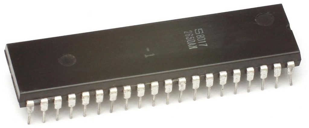
In mid 2015, once I had got the emulator sort of working, I happened upon an arcade/pinball repairer on the Aussie Arcade website who was selling some of his stock of the Philips/Valvo variant of the Signetics 2650, the MAB2650, so I purchased a couple. Also at this time I was interested in the Retrobrew Computers site which had developed many CPU, I/O boards and backplanes in a Eurocard Bus format. The attraction here is that they tend to use old school through hole components for their boards which is great for my old eyes and a retro feel.
So, fast forward to 2018, after a couple of moves and a lot of hand sitting, I finally started thinking about getting one of the MAB2650 CPUs into a circuit. Whilst there are a few designs from the 70’s that I could have just built up, I decided that I would like to have some flexibility to my design and use some more modern components, while still keeping to the through hole designs of the Retrobrew Computers group. I thought of making up a standalone CPU card similar to the SBC V2, that could be used standalone or work with the ECB backplane, to interface with several of the ECB I/O boards that had been developed by the crew at Retrobrew Computers.
To be able to do this, I used some of the basic schematic elements and features available on the SBC V2 board and used some glue logic to match the signals for the ECB backplane. The 2650 has an extended I/O bus with 256 ports which is similar to the Z80, and so seems quite easy to match the signals to the ECB bus.
Some design goals and specifications:-
- Interface the 2650 control signals to match Z80 control signals, and thus use the ECB bus and peripherals;
- 32Kbytes of RAM, with the possibility of a paging system to increase available RAM at a later time;
- Be able to use from 1Kbyte to 8Kbyte images in an 8K EEPROM/Flash. Then I can load the different boot ROMs available for the 2650 and also develop my own software; and
- Be able to software switch the ROM out of circuit via a latch, similar to how CPM systems work.
Using these goals would hopefully give me the flexibility I wanted out of this board. So, jumping into to KiCAD for the first time, I got to work on the schematic.
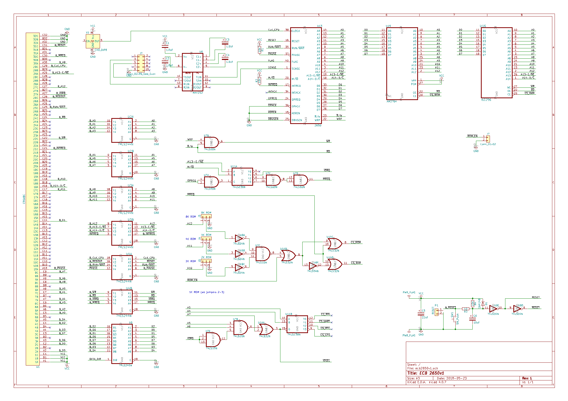
Across the top of the schematic is the CPU with a 1MHz oscillator and the MAX232 for serial comms, the 8K EEPROM/Flash and 32Kbytes of RAM. Down the left hand side is the ECB connector and ECB buffers. Just below the CPU is some logic to deal with translating the 2650 signals into Z80 style signals. Below that is the address decoding for Rom and RAM, and below that some thoughts on future I/O decoding. Off to the bottom right is the reset circuit.
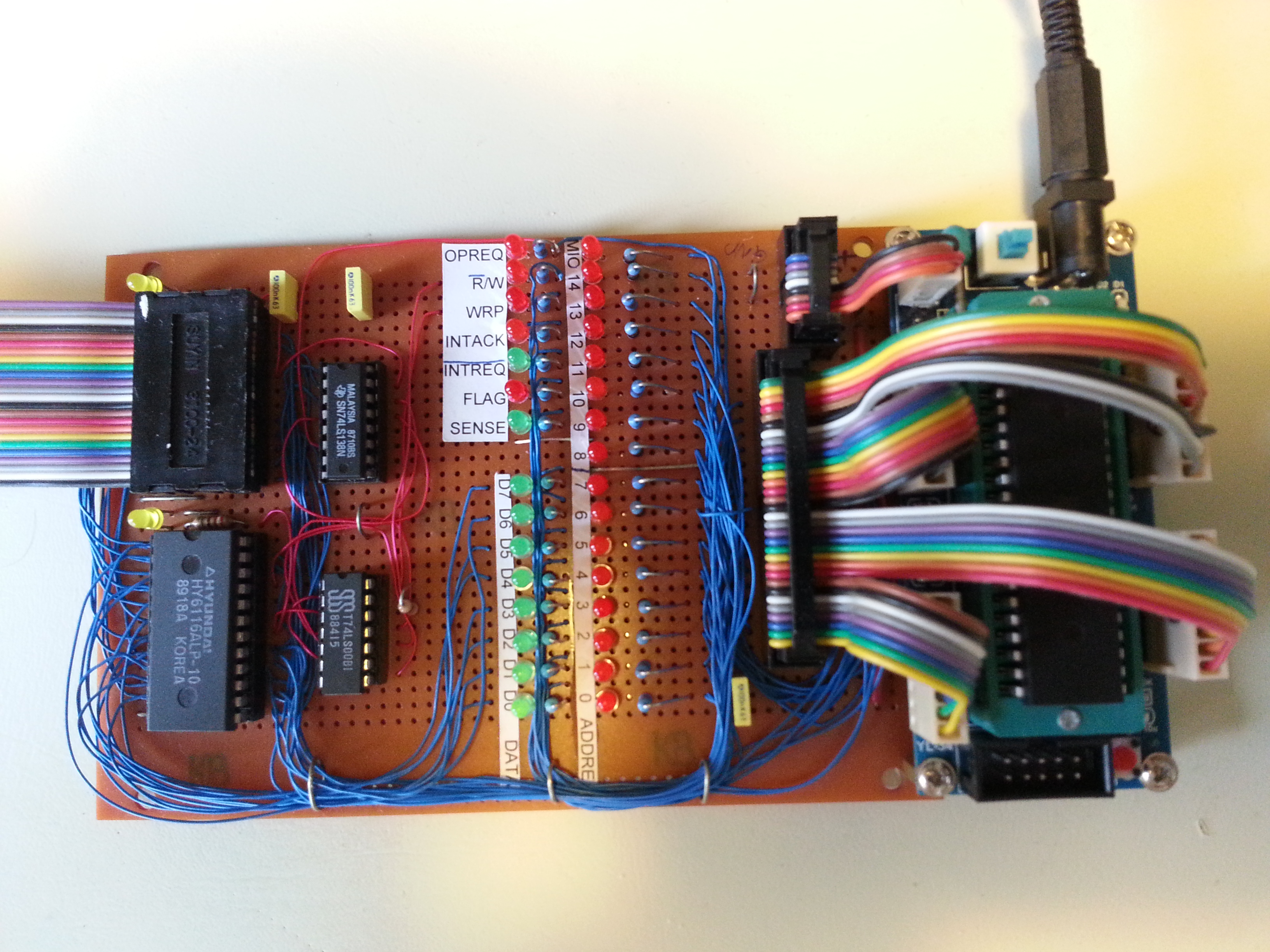
I tried to build up some of the schematic on a breadboard to test it, but had issues with getting it going, mainly due to what I thought at the time was poor breadboard connections. So I managed to only test out some of the basic logic ideas and thought that my design was reasonably solid, and so at this point I committed to a prototype build which wouldn’t be as susceptible to poor breadboard type connections.
In Part 2, I’ll construct the prototype board and later find a problem with the design…..