
So, in Part 2 we found an issue where the ROM address space was reappearing in the memory map when it wasn’t meant too. I thought I’d try and use an excel spreadsheet to formulate the logic on the board and verify the design, and was able to put in a hex address and see the logic change. With this I soon found the problem with the design.
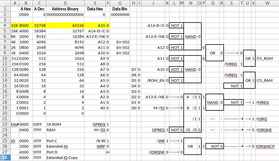
In my haste to get a design which allowed different sized ROM images to work in an 8Kbytes EEPROM/Flash device, I neglected to properly test the addressing logic. The answer of course is I didn’t take into consideration the proper states of A13 and A14, which is why the ROM is appearing to repeat itself through the memory map. Obviously my (brief and flawed) testing didn’t pick this up.
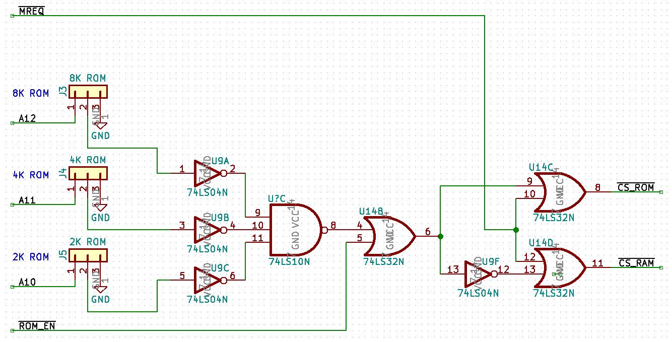
You will notice that in the spreadsheet above, I have added the A13 and A14 address lines, to make the logic work properly, and it does what I intended. However this presented another problem. To make this happen, I needed 2 new NOT gates. To do this I needed another 74LS06 (or other free gates that could be used as a NOT) to make up the needed logic. How was I going to do this with my already populated prototype? I had no room left. Sure, I could add an extra piece of board, turn the chip upside down and just wire it in. But doing this kind of hack was ugly. A bit of thought was needed.
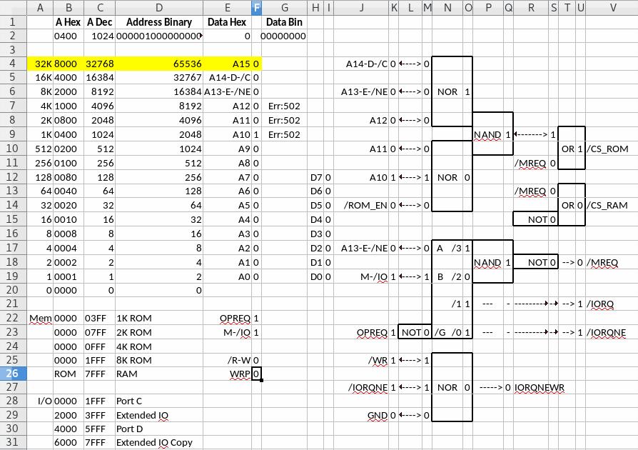
Enter spreadsheet logic design V2. I found that by using 3-input NOR gates instead of the NAND gates, allowed me to eliminate the NOT gates on the address lines and save myself from adding an extra chip.
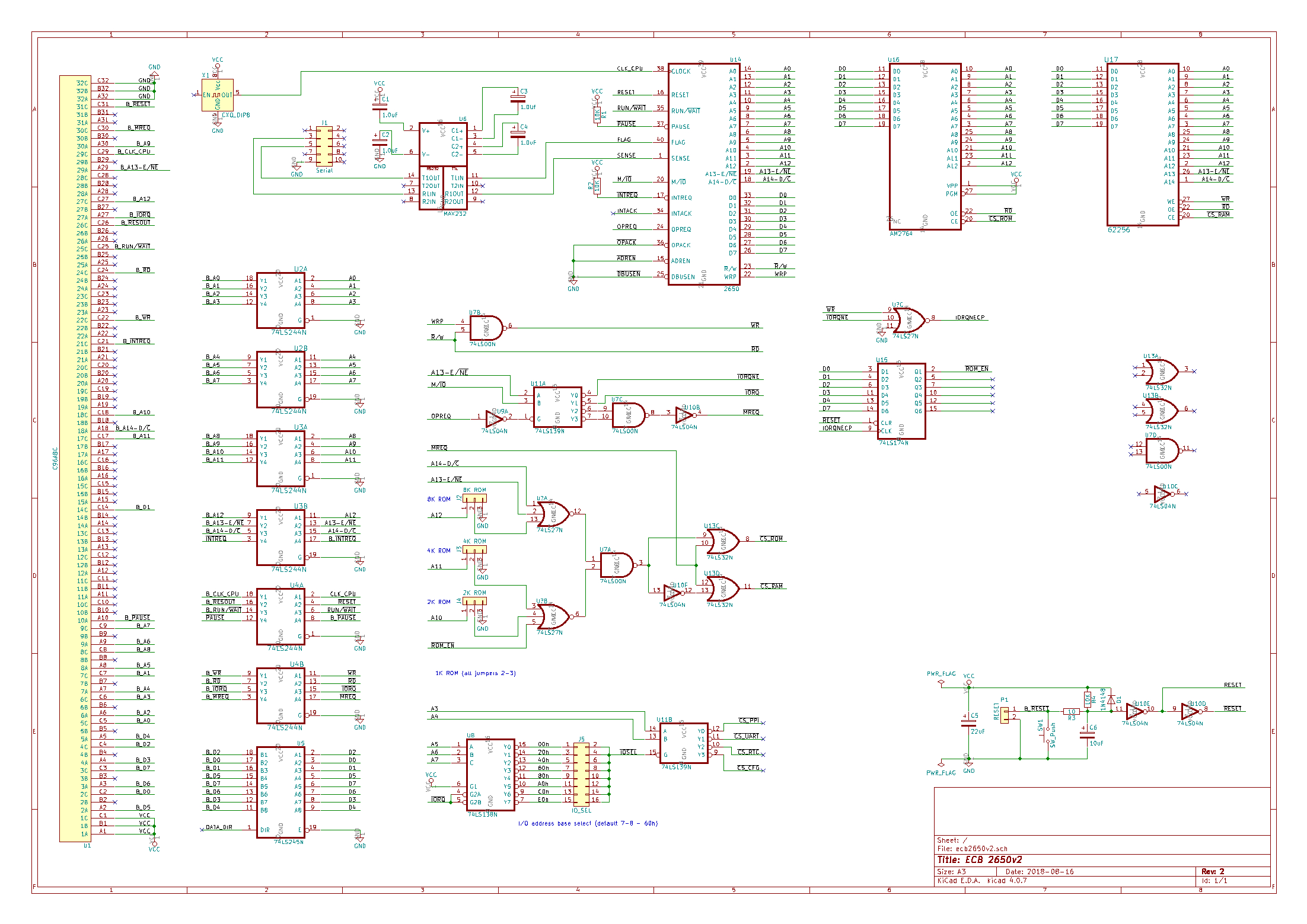
Above is the new V2 design, and I have properly tested this using the spreadsheet I developed. Some would say this is what I should have done the first time round, but you live and learn. The CPU, EEPROM and RAM section and the ECB buffers are the same. I have been able to replace the 74LS10 3x 3-input NAND gate chip with a 74LS27 3x 3-input NOR gate chip. I have moved some gates around now that I have a few spare, and I have added some better on-board I/O addressing and a latch for the ROM enable/disable control. Rather than just using a single latch for this purpose, I would use a 6 gate flip flop IC which will give me some future expandability, possibly RAM paging.
Now, onward to modify the prototype.
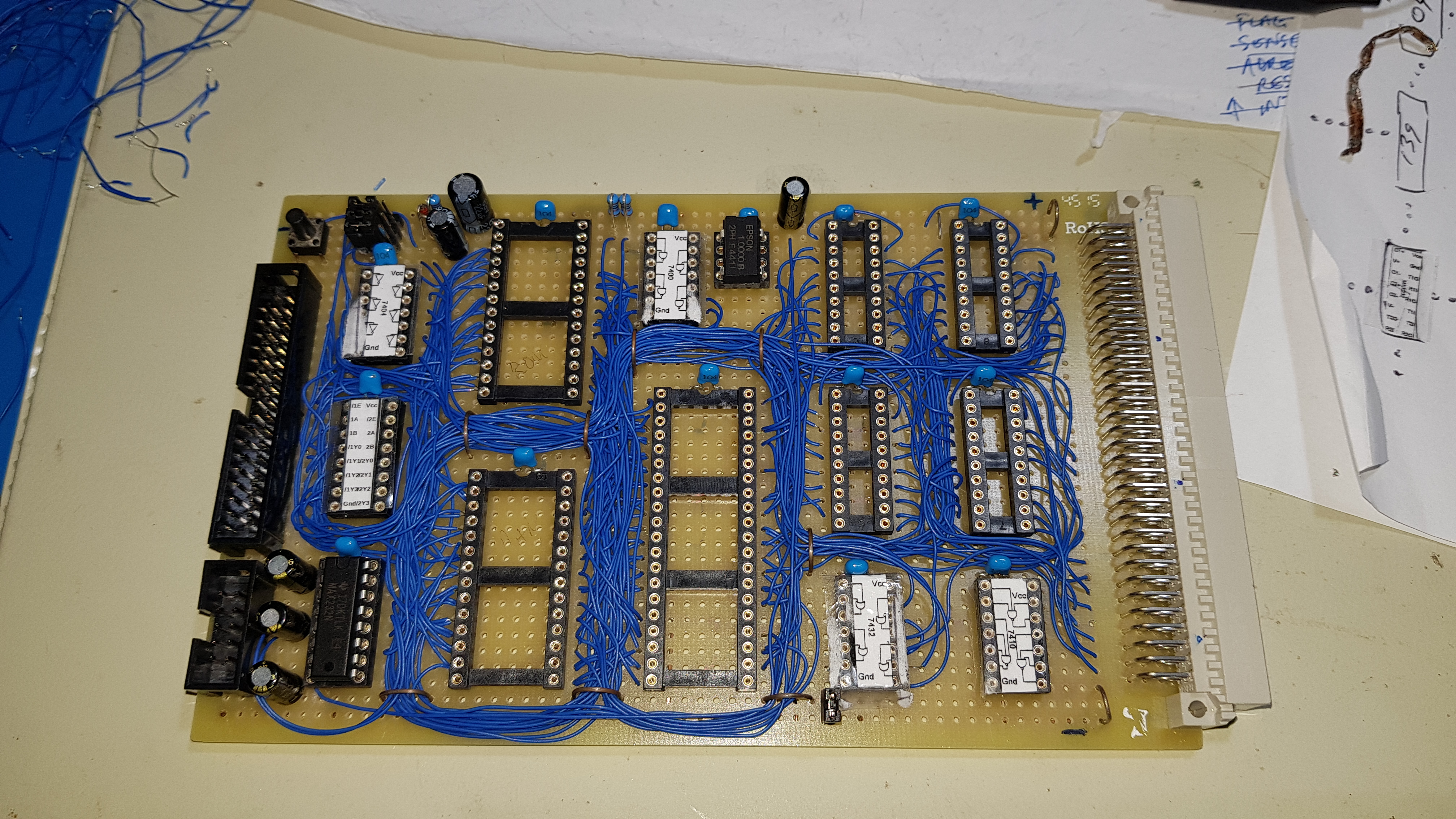
I put back on some of the labels to help with wiring again and ripped out the wires that were incorrect. I used the old 74LS10 label, as it has the same internal connections as a 74LS27 NOR gate and wired it up according to the KiCAD schematic.
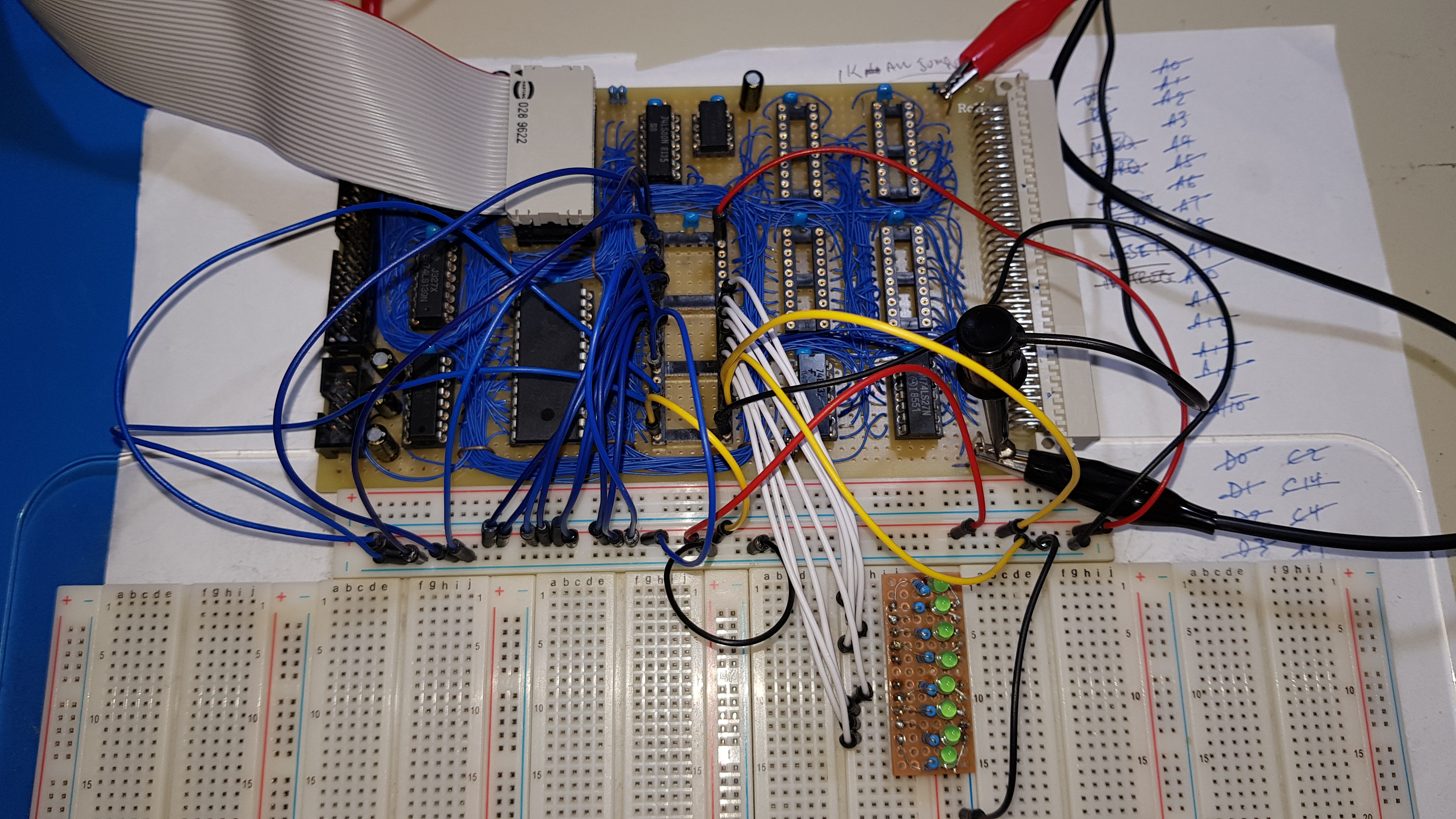
I used the test rig again to just check my logic functionality and all seems fine. So I plug in the CPU again and fire it up. Woohoo, PIPBUG console prompt. I load and run the memory test program once again and all the RAM this time checked out correctly. Time to test it out with a few other programs from the Electronics Australia magazines.